This tutorial will introduce you to VHDL design on the Spartan 3 FPGA board that you will use for the exercises in this part of the course.
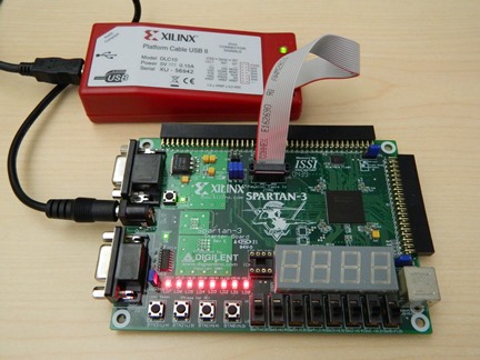
The first step is to ensure that the JTAG programming cable is connected between a USB port on the development station USB port and the two-row JTAG connector on the Spartan 3 FPGA board. The red stripe on the flat ribbon cable goes to pin 1 which is on the left side of the connector. Be careful to line up the flat ribbon connector and not skip any pins. Next, plug in the power cord between the VGA and serial port connectors. You will program the device through the USB cable adapter connected to the JTAG port..
The Xilinx ISE works with projects. All the files for one project are stored in a directory. You can place this directory anywhere. If you want to create a directory in your Z: drvie to hold all of your Xilinx projects you can do that now.
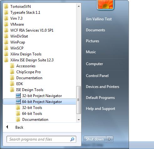
Start the Xilinx ISE Project Manager. There are two versions of the Xilinx tools on the development workstation, use the 12.3 verison of the tools. If you get a warning about not finding the license manager, start the Xilinx license manager tool and on the License Manage tab enter the LM_LICENSE_SERVER information that your instructor gives you.
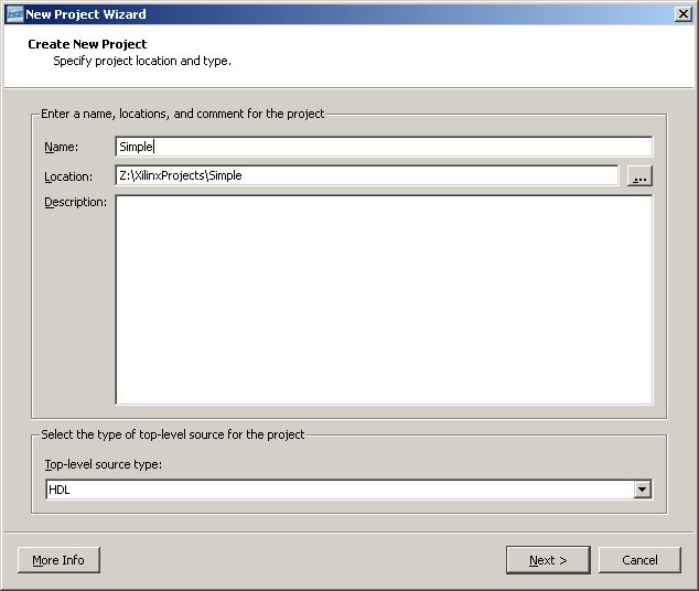
In the example here, all Xilinx projects are placed in the directory z:\XilinxProjects. To begin a new project, select File -> New Project. Complete the fields for a project named Simple which is an HDL type.
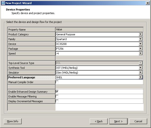
You will next have to define the properties for the FPGA device you will work with. The top section of the dialog box must be modified from the default values. You want a General Purpose, Spartan 3 family, XC3S200 device, in a FT256 package. The speed rating is 4. Also, specify the preferred language as VHDL.
When you are given the option to create a new source file click on the New Source button.
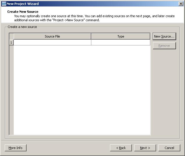
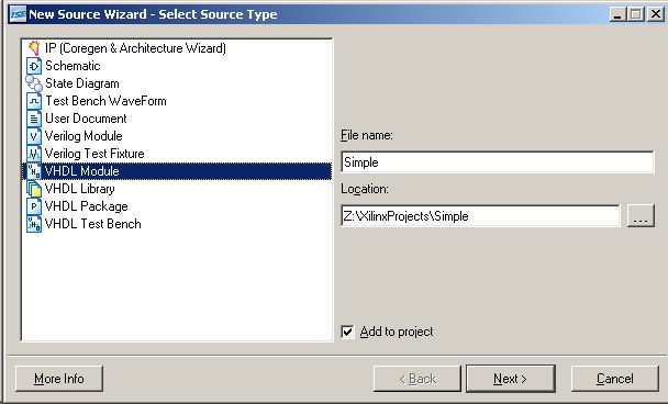
Since this project is called Simple use that as the name for a VHDL Module. Make sure that the Location is somewhere in your Z drive and that you check the Add to project checkbox.
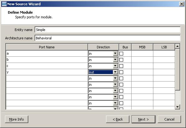
Now define the module inputs and outputs. To start we want three inputs (a, b, c) and one output (y).
Now click through the Summary, Create New Source, and Add New Source dialogs using Finish or Next buttons. You will eventually get to the display of the full project summary. In a second tab, you should see the Simple.vhd file.
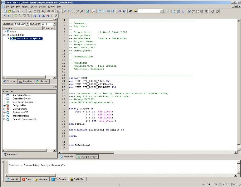
After the initial comment header, make sure that the library usage includes all of the following lines:
library IEEE;

		use IEEE.STD_LOGIC_1164.ALL;

		use IEEE.STD_LOGIC_ARITH.ALL;

		use IEEE.STD_LOGIC_UNSIGNED.ALL;
In this file, you will see the entity and architecture sections of the VHDL file. The module inputs and outputs have been defined for you in the entity section. Behavior description goes between the begin and end statements in the architecture section. Add this simple statement of behavior for this device:
y <= a and b or c;
Save this change. Now process this file by highlighting the VHDL file in the Source Hierarchy. Right click on Synthesize - XST in the Processes section in the lower lefthand corner and select Run. If you entered the statement exactly as shown above, you will get an error message in the lower window. You can get some additional help which is sometimes useful. In this case, it is not very helpful because the problem is not with a semicolon. The error is that the and and or operators are at the same level of precedence and the tool wants a statement of explicit precedence. Place parentheses around a and b and the error should go away when you rerun the synthesis tool.
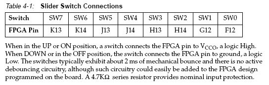
Next, you need to describe what your module inputs and output are connected to. In this case, they go to device pins and then on the Spartan 3 board to the switches and LEDs. The Spartan 3 Reference Manual contains all the information you need about the connections to the FPGA device. Here is how the switches are connected.
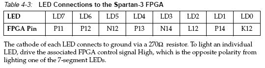
And for the y output, here are the pin assignments for the LEDs.
This pin connection information goes into a constraints file. It is easiest to create this file by creating a new file as a text file (File -> New then select Text file). Take a look at the tables above and these pin connections to see the correspondence with siwtches and an LED on the FPGA board. Copy these pin connections into the text file.
NET "a"   LOC = "F12";
NET "b"   LOC = "G12";
NET "c"   LOC = "H14";
NET "y"   LOC = "K12";
Save the file as Simple.ucf in the same directory where Simple.vhd is located. Now add it to your project by right clicking Simple – Behavorial (Simple.vhd) in the sources tab, and select Add Source to add Simple.ucf.
Right click Implement Design select run. (You may need to highlight the VHDL source file if you do not see all the process options.) Right click Generate Programming File and select Run.
Right click Configure Target Device; and select Run. Use OK to dismiss any warning about not having an Impact file specified. After a period, sometimes a very long one, the ISE iMPACT window should appear.
Double click the Boundary Scan in the iMPACT Flows area in the upper left corner. Click the Initialize Chain toolbar button (four green boxes with chain connecting) or
You should see a diagram with two device boxes. One is the FPGA and the other is the flash memory used to program the FPGA at startup. You will always be programming the FPGA. It should be highlighted in green. (If not, cancel the operations so that you can click the device picture to highlight the xc3s200. Then right click the device and select Assign New Configuration File ...)
Answer Yes to assign configuration files.
You should see the FPGA device (xc3s200) highlighted in green. In the Assign New Configuration File look in your Simple directory and select simple.bit to open.
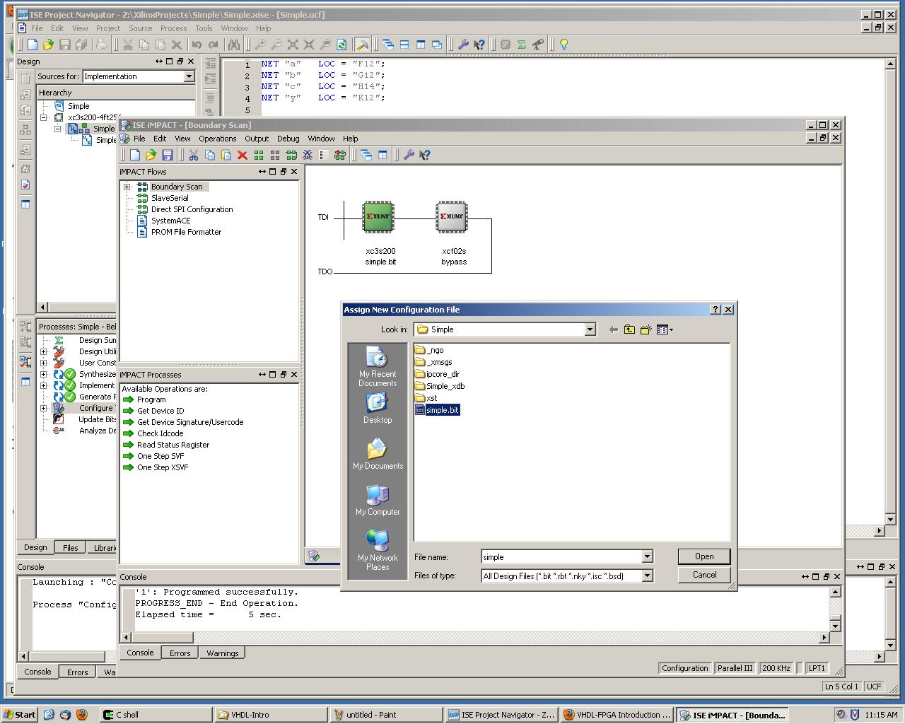
Bypass setting a configuration file for the flash memory (xcf02s).
Click OK on the Device Programming Properties dialog.
Right click the FPGA device, select Program. If the programming is successful, verify that the rightmost LED correctly lights as the output of the logic expression using the three rightmost slide switches as the inputs.
Now you will add a clock into the logic.
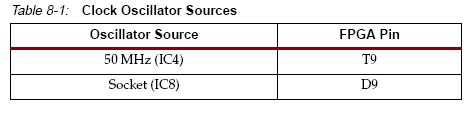
Start by defining the 50 MHz clock as an input to this module. Adding mclk : in std_logic; to the entity section should do the trick. You will also need to define two signals that are internal to the architecture. Add these two lines just above the begin statement in the architecture section.
signal cclk : std_logic;signal clkdiv : std_logic_vector(23 downto 0);
Now add to the architecture this process statement that will divide down the clock and make a lower frequency signal available to the logic by counting rising edges of the clock, and using bit 23 as a divided down, lower frequency signal.
-- Divide the master clock (50Mhz) down to a lower frequency.
process (mclk)
  begin
    if rising_edge(mclk)then
      clkdiv <= clkdiv + 1;
    end if;
end process;
cclk <= clkdiv(23);
Use the lower frequency signal to blink the LED output when it is on. Do that by modifying the logic to
y <= cclk and ((a and b) or c);
You also have to add the pin description for the 50 MHz clock to the UCF file. Here is the information that you need.
Save all your changes. Synthesize, Implement, Generate and Program. Select yes when asked to reload the bit file. Check that you have a flashing LED.
The last etude will be displaying a four bit binary value in hex on the seven segment display. Here are the steps that you will need to do:
switches use the syntax signal<#> in the UCF NET statement, such as, NET "switches<3>" LOC "H13".segments <= "0111111" when switches = "0000" else.You now should have enough of a base to tackle the Individual VHDL assignment.